


In VLSI (Very Large Scale Integration) design, clock gating is a technique used to reduce power consumption by selectively disabling the clock signal to parts of a circuit when they are not in use. This is crucial in modern digital circuits, especially for battery-powered devices or energy-efficient systems. Clock gating ensures that the circuit does not waste power by activating unused portions of the system, making it a powerful tool for power optimization.
How Does Clock Gating Work?
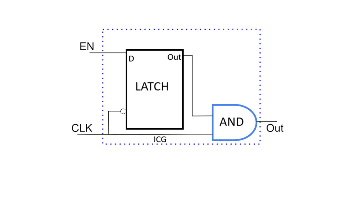
In a typical digital circuit, the clock signal drives sequential elements like flip-flops and registers, updating their states on each clock cycle. However, not all parts of a circuit need to be active all the time. Clock gating works by blocking the clock signal from reaching specific sequential elements during idle times.
- Control Signal: A control signal (enable signal) determines when to disable the clock for a particular section.
- Gating Logic: Logic gates, often AND gates, are used to control whether the clock signal is allowed to pass through.
- Disabled Sections: When the control signal is low, the clock is blocked, and the sequential elements do not change their state.
Key Benefits of Clock Gating in VLSI Design
- Power Savings: Clock gating helps significantly reduce dynamic power consumption, which is the power used when the circuit actively switches. By disabling the clock in idle sections, the system consumes less energy.
- Efficiency: Clock gating optimizes the overall energy efficiency of a circuit, particularly in low-power applications like mobile devices, IoT devices, and wearables.
- Reduced Switching Activity: Since sequential elements are not toggled when unnecessary, switching activity is reduced, leading to less power consumption and heat generation.
Types of Clock Gating
- Manual Clock Gating: Designers can manually insert clock gating logic to disable the clock in unused parts of the circuit. This requires careful analysis to ensure critical sections are not inadvertently gated.
- Automatic Clock Gating: Many EDA (Electronic Design Automation) tools can automatically insert clock gating logic based on circuit behavior, optimizing power usage without manual intervention.
Components of Clock Gating
- Control Signal: This enables or disables the clock based on certain conditions.
- Clock Gating Logic: Typically, an AND gate or other gating logic is used to selectively pass the clock signal to the sequential elements.
- Sequential Elements: Flip-flops, latches, or registers are the primary targets of clock gating. These elements retain state and are clock-driven.
Applications of Clock Gating in VLSI Design
- Low-Power Devices: Clock gating is widely used in battery-powered devices like smartphones, wearables, and laptops, where power consumption is a key concern.
- Multi-core Processors: In multi-core systems, clock gating can turn off the clock to idle cores, saving power when cores are not being used.
- Idle Modules: In systems with burst processing (such as communication or video processing), clock gating can disable the clock in idle modules to save energy when the system isn’t actively processing data.
Clock Gating Logic Example
Consider a scenario where a flip-flop or register doesn’t need to update its state continuously. The clock signal is gated using an AND gate, with the control signal determining when the clock should be passed through. If the control signal is low, the clock is blocked, and the flip-flop’s state remains unchanged, saving power.
Clock Gating Logic Diagram:
            +---------+
Clock ---> | AND Gate | ---> Clock to Flip-Flop
            +---------+
                  ^
                  |
          Control Signal (Enable)
Advantages of Clock Gating
- Significant Power Reduction: By disabling clocks to inactive sections, power consumption is greatly minimized.
- Energy Efficiency: Clock gating is a fundamental technique for energy-efficient circuit design, crucial for devices with limited battery life.
- Improved Circuit Reliability: Reduced power consumption also leads to less heat generation, contributing to the long-term reliability of the circuit.
Challenges of Clock Gating
- Increased Design Complexity: Inserting clock gating logic requires careful consideration to ensure the circuit functions correctly. It involves a timing analysis to prevent any undesirable side effects.
- Clock Skew: Adding clock gating logic can cause clock skew or timing violations. This is especially critical in high-speed circuits, where accurate synchronization is required.
- Additional Overhead: The clock gating logic itself introduces some area and performance overhead, adding gates and signals to the design.
Clock Gating vs. Other Power Optimization Techniques
While clock gating is highly effective, it is just one of several techniques used for power optimization in VLSI design. Other methods, such as dynamic voltage and frequency scaling (DVFS), power gating, and low-power design techniques, can be used in conjunction with clock gating for more comprehensive power savings.
Conclusion: The Importance of Clock Gating in Modern VLSI Design
In VLSI design, clock gating plays a critical role in optimizing power consumption, particularly in battery-operated or power-sensitive devices. By selectively disabling the clock signal to idle sections of the circuit, clock gating helps reduce dynamic power, improve energy efficiency, and extend the life of portable devices. Though it adds complexity to the design process, the power-saving benefits make it an indispensable tool for modern VLSI systems.
Incorporating clock gating into your VLSI designs ensures optimal performance while balancing power efficiency, making it a key technique in the creation of low-power, high-performance digital circuits.


