June 27, 2025

Static Timing Analysis

Static Timing Analysis

STATIC TIMING ANALYSIS [STA]: OCV vs AOCV vs POCV

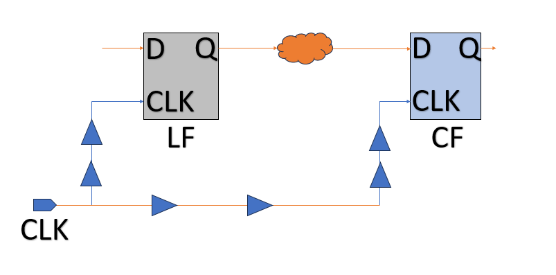
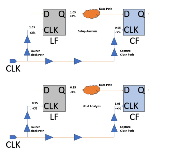
In VLSI design, OCV (On-Chip Variation), AOCV (Advanced On-Chip Variation), and POCV (Process On-Chip Variation) refer to methods and models used for accounting for variations in the manufacturing process that affect the performance of a chip. These variations are critical to ensure the robustness and performance of the chip under varying operating conditions and manufacturing tolerances. Here’s a breakdown of each

Read More
Static Timing Analysis

STATIC TIMING ANALYSIS [STA]: Optimization of Timing Violations in VLSI

Optimizing for timing violations in VLSI (Very-Large-Scale Integration) involves various strategies to ensure the chip operates within its specified timing requirements, particularly in SoC (System-on-Chip) designs where multiple components and clock domains must synchronize. Here’s an optimized approach to handle timing violations: 1. Types of Timing Violations 2. Strategies for Timing Violation Optimization Strategy Description Pipelining Breaking

Read More
Static Timing Analysis

Static Timing Analysis [STA]: Timing Paths in STA for VLSI: A Complete Guide

Static Timing Analysis (STA) is a critical process in VLSI design that is used to validate the timing of a circuit. It ensures that the signals within the circuit propagate correctly and meet the required timing constraints. One key element of STA is the analysis of timing paths, which are the paths that signals take between flip-flops,

Read More
Static Timing Analysis

Static Timing Analysis [STA]: Clock Skewing [Clock Push (Late Skew) and Clock Pull (Early Skew)]​

Concept of Useful Skew We will first explore the fixes for setup violations, which involve only data path optimization: Once we have exhausted data path optimization options, we will go for clock skewing as it involves touching of high fanout clock network. Now, let us say, the timing path from LFF to CFF (refer to the given diagram) is violating hold. We will first explore the

Read More
Static Timing Analysis

STATIC TIMING ANALYSIS [STA]: What is Clock Gating in VLSI? A Key Technique for Power Optimization

In VLSI (Very Large Scale Integration) design, clock gating is a technique used to reduce power consumption by selectively disabling the clock signal to parts of a circuit when they are not in use. This is crucial in modern digital circuits, especially for battery-powered devices or energy-efficient systems. Clock gating ensures that the circuit does not waste power by activating unused portions of the

Read More
Static Timing Analysis

STATATIC TIMING ANALYSIS [STA]: Key differences between Combinational Cells and Sequential Cells in VLSI Design

In VLSI (Very Large Scale Integration) design, the core components of digital circuits are often built using two types of fundamental cells: combinational cells and sequential cells. These cells serve as the building blocks for complex logic operations in integrated circuits. While both types are essential in VLSI circuits, they function in significantly different ways. Let’s take a deeper

Read More
Static Timing Analysis

STATIC TIMING ANALYSIS [STA]: Order of Fixes During ECO Cycle in VLSI

ECO, or Engineering Change Order, is a vital step in the VLSI design flow, allowing engineers to implement fixes and optimizations at various stages of the design cycle. As modern chip designs grow increasingly complex, ECO plays a crucial role in ensuring design closure with minimal impact on cost, time, and resources. Here is a

Read More
Static Timing Analysis

STATIC TIMING ANALYSIS [STA]: How to Fix Setup Violations

Static Timing Analysis (STA) is crucial for verifying the timing behavior of digital circuits in ASIC and FPGA designs. One common issue during STA is the setup violation, which occurs when data does not meet the setup time requirement before a clock edge, leading to incorrect results. What is a Setup Violation? A setup violation happens when the

Read More
Static Timing Analysis

Static timing Analysis [STA] : Register Retiming

Register Retiming is an optimization technique used in digital circuit design to improve performance, reduce power consumption, or minimize area. It involves moving registers across combinational logic gates without changing the circuit’s functionality. Purpose of Retiming 1. Increase Clock Speed (Reduce Critical Path Delay) By redistributing registers, retiming can balance logic delays and reduce the

Read More