


Physical design in VLSI (Very Large Scale Integration) refers to the process of converting a high-level logical design into a physical layout that can be fabricated on a semiconductor chip. It involves arranging, placing, and routing components on a chip to meet power, performance, and area (PPA) requirements, ensuring efficient design and manufacturability.
Key Steps in Physical Design of VLSI
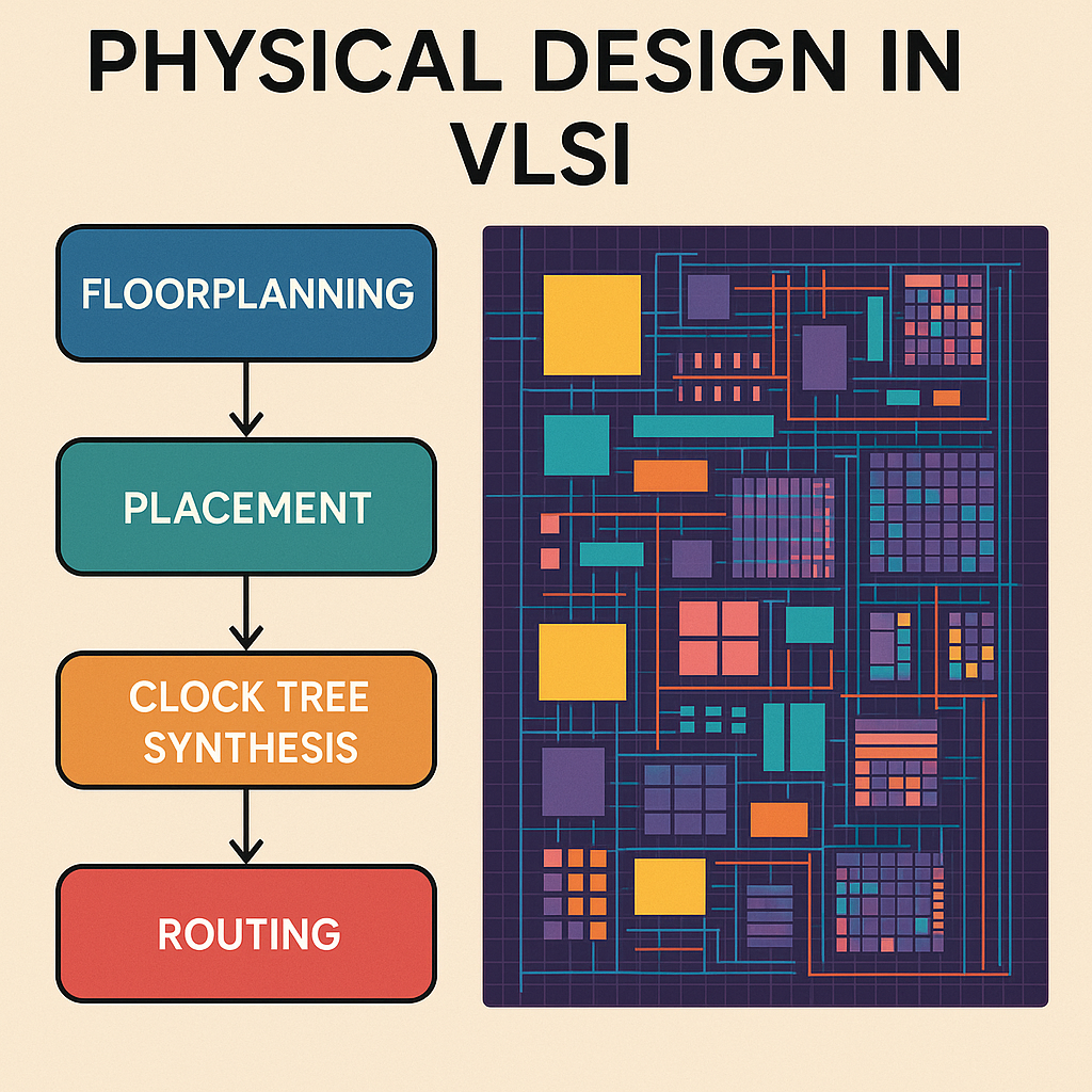
- Floorplanning:
- Floorplanning is the first step where major functional blocks [Macros] are placed in a manner that minimizes delay, improves performance, and ensures power distribution.
- It includes decisions about block size, interconnects, clock distribution, and power grids.
- Placement:
- Placement determines the exact positions of the individual standard cells (gates, flip-flops) within the floorplan.
- The goal is to minimize wire length, reduce delays, optimize power and area, and ensure design rule compliance.
- Clock Tree Synthesis (CTS):
- Clock Tree Synthesis (CTS) involves constructing and distributing the clock signal uniformly across the chip.
- Proper CTS minimizes insertion delay, clock skew, and ensures all flip-flops receive the clock signal simultaneously.
- Routing:
- Routing involves connecting the placed cells with metal layers for signal, power, and ground distribution.
- Global routing finds the general path, while detailed routing connects the exact paths for signals.
- Design Rule Checking (DRC):
- DRC ensures the layout adheres to the manufacturing process rules, checking spacing, widths, and other constraints to avoid design errors.
- Layout vs. Schematic (LVS) Check:
- LVS compares the layout to the original schematic to verify that the physical design matches the logical design.
- It detects errors such as missing connections or incorrect device placements.
- Parasitic Extraction:
- Parasitic extraction identifies parasitic components like resistance, capacitance, and inductance that could affect signal integrity.
- These parasitics must be accounted for to ensure accurate delay and performance prediction.
- Sign-off:
- After all checks, the design enters the sign-off stage, which includes timing analysis, power analysis, and signal integrity checks to ensure the chip is ready for manufacturing.
Importance of Physical Design in VLSI
- Performance Optimization:
- Physical design ensures that the chip meets performance requirements by minimizing delays and optimizing wire routing.
- Area Efficiency:
- Optimizing the layout ensures efficient use of the silicon area, allowing for high-density integration of logic gates and components.
- Manufacturing Feasibility:
- Physical design must adhere to the constraints of the fabrication process, ensuring the design can be successfully manufactured without defects.
- Power Efficiency:
- Proper routing and placement minimize power consumption, crucial for battery-powered devices like smartphones and IoT devices.
Challenges in Physical Design
- Design Rule Violations:
- Ensuring compliance with design rules is a major challenge as chip designs grow more complex. Violations can prevent manufacturing or result in functional errors.
- Timing Closure:
- Achieving timing closure ensures that all timing constraints (such as clock arrival times) are met, a complex task in modern VLSI designs.
- Power and Thermal Management:
- Managing power distribution and thermal issues is crucial for high-performance chips to prevent overheating or damage.
- Complexity of EDA Tools:
- The complexity of Electronic Design Automation (EDA) tools required for physical design needs skilled engineers and often involves multiple iterations to achieve optimal results.
Benefits of Physical Design in VLSI
- Optimized Power, Performance, and Area (PPA):
- Physical design allows engineers to balance PPA requirements, ensuring the chip performs well, uses power efficiently, and fits within a compact area.
- Increased Chip Reliability:
- Proper routing and placement minimize signal interference and heat buildup, improving the overall reliability of the chip.
- Faster Time to Market:
- Efficient physical design streamlines the process, reducing the time it takes to bring a product to market and enabling faster prototyping.
Physical Design Tools Used in VLSI
- Floorplanning and Placement Tools: Tools like Synopsys IC Compiler and Cadence Innovus are widely used for initial design layout and placement optimization.
- Routing Tools: These tools ensure that signal paths are optimized, such as Mentor Graphics Olympus and Cadence Encounter.
- DRC and LVS Tools: Tools like Calibre are used for design rule checking and verifying the layout against the schematic.
Conclusion: The Role of Physical Design in VLSI
In VLSI design, physical design plays a crucial role in transforming a logical circuit description into a manufacturable chip layout. It involves multiple steps like floorplanning, placement, routing, and various checks (such as DRC and LVS) to ensure optimal performance, power efficiency, and manufacturability. As VLSI designs continue to increase in complexity, the role of physical design becomes even more critical in ensuring that chips meet their specifications and are ready for efficient, reliable mass production.


Leave feedback about this