
![STATIC TIMING ANALYSIS [STA]: Optimization of Timing Violations in VLSI](https://anuthipahal.com/wp-content/themes/neeon/assets/img/noimage.jpg)


Optimizing for timing violations in VLSI (Very-Large-Scale Integration) involves various strategies to ensure the chip operates within its specified timing requirements, particularly in SoC (System-on-Chip) designs where multiple components and clock domains must synchronize. Here’s an optimized approach to handle timing violations:
1. Types of Timing Violations
- Setup Time Violation: This occurs when the data is not stable at the input of a flip-flop before the clock edge.
- Hold Time Violation: Happens when the data input changes too soon after the clock edge.
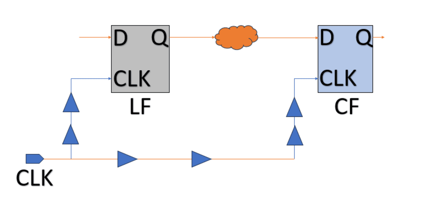
- Clock Skew Violation: When there’s a delay difference between different parts of the clock network, leading to misalignment.
- Propagation Delay Violation: Caused by excessive delay in the signal propagation across a logic path.
2. Strategies for Timing Violation Optimization
| Strategy | Description |
|---|---|
| Pipelining | Breaking long combinational paths into smaller stages, reducing delay and mitigating violations. |
| Clock Gating | Disabling unused portions of the circuit, reducing dynamic power, and improving timing by removing unnecessary logic. |
| Logical Restructuring | Rewriting the logic or adding gates to improve timing, such as reducing the number of gates or optimizing gate delays. |
| Buffer Insertion | Placing buffers or repeaters in the signal path to reduce load capacitance and improve signal propagation speed. |
| Retiming | Repositioning registers along critical paths to balance delays and reduce the overall critical path length. |
| Parallelism | Increasing the number of parallel paths to reduce delays on any single critical path. |
| Optimized Floorplanning | Placing critical components and timing-sensitive logic closer to minimize routing delays. |
| Clock Tree Synthesis (CTS) | Proper clock tree design to minimize skew and latency. Balancing the clock tree helps prevent timing violations due to unequal clock distribution. |
| Technology Scaling | Leveraging smaller process nodes (e.g., 7nm, 5nm) with faster transistors and lower capacitance, improving overall timing. |
3. Tools for Timing Optimization
- Static Timing Analysis (STA): Essential for identifying timing violations and areas for optimization (e.g., Synopsys PrimeTime, Cadence Tempus).
- Place & Route Tools: Tools like Innovus or ICC2 or Fusion Compiler help with placement optimization to reduce path delays.
- Clock Tree Synthesis (CTS) Tools: Tools like Cadence Encounter CTS and Synopsys Fusion Compiler improve the clock distribution network, reducing skew and timing issues.
4. Common Timing Violation Fixes
- Reduce Long Critical Paths: Use pipelining and retiming to split long logic chains.
- Increase Clock Period: If possible, adjust the clock period to allow more time for data to propagate.
- Improve Routing: Optimize wire lengths and reduce resistance and capacitance to improve signal propagation.
- Resize Transistors: Change the size of transistors to balance speed and area trade-offs.
5. Timing Analysis and Signoff
Once optimizations are made, ensure the chip passes signoff using comprehensive tools like PrimeTime or Tempus to verify that all timing violations are resolved and the design meets all constraints.
6. Best Practices
- Iterative Design: Continuously run timing analysis throughout the design process, especially after each optimization step.
- Test with Corner Cases: Check timing under worst-case conditions (e.g., voltage variations, temperature extremes) to ensure reliability.
- Cross-Check Clock Domains: In SoCs, ensure proper handling of clock domain crossings (CDC) to avoid violations between different clock domains.
By carefully applying these techniques, you can efficiently optimize timing violations and ensure that the design meets the desired performance and timing requirements.


Leave feedback about this