
![Static Timing Analysis [STA]: Timing Paths in STA for VLSI: A Complete Guide](https://anuthipahal.com/wp-content/themes/neeon/assets/img/noimage.jpg)


Static Timing Analysis (STA) is a critical process in VLSI design that is used to validate the timing of a circuit. It ensures that the signals within the circuit propagate correctly and meet the required timing constraints. One key element of STA is the analysis of timing paths, which are the paths that signals take between flip-flops, registers, and other components in the design.
Key Concepts in Timing Path Analysis
- Setup Time: The time before the clock edge that data must be stable for it to be captured correctly.
- Hold Time: The time after the clock edge that the data must remain stable to be reliably captured.
- Clock-to-Q Delay: The delay between the clock edge and the output of a flip-flop.
- Propagation Delay: The delay of signals passing through logic gates and interconnects.
- Max Delay (Tmax): The maximum time a signal can take before failing the setup requirement.
- Min Delay (Tmin): The minimum time a signal needs to remain stable after a clock edge to meet the hold time.
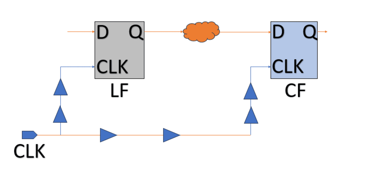
Types of Timing Paths in STA
- Setup Path: Ensures data is correctly captured at the next clock cycle. The setup path includes the flip-flop’s output, the combinational logic, and the next flip-flop input. Setup Timing Equation: Clock Period + Clock Skew ≥ Clock-to-Q Delay of Launch Flop + Combinational Path Delay + Library Setup time of Capture flop
- Hold Path: Ensures the data remains stable after the clock edge. This path checks for timing issues after the flip-flop captures the data. Hold Timing Equation: Clock-to-Q Delay of Launch Flop + Combinational Path Delay ≥ Clock Skew + Library Hold time of Capture flop
Steps for Timing Path Analysis in STA
- Identify Timing Paths: Determine all possible paths from flip-flops through combinational logic to the next flip-flop. Consider both setup and hold timing paths.
- Calculate Path Delays: Compute the propagation delays of signals through logic gates, flip-flops, and interconnects.
- Check Setup Timing: Compare the setup path delays with the clock period. If the delay exceeds the clock period, the setup timing fails.
- Check Hold Timing: Ensure the data remains stable long enough after the clock edge to meet the hold time.
- Slack Calculation:
- Setup Slack: The difference between the required setup time and the actual signal arrival time. Negative slack means a timing failure.
- Hold Slack: The difference between the required hold time and the actual signal stability. Negative hold slack indicates a failure.
Example Timing Path Calculation
Consider the following parameters:
- Clock Period = 10ns
- Clock-to-Q Delay = 2ns
- Combinational Path Delay = 5ns
- Setup Time = 3ns
- Hold Time = 1ns
Setup Check:
Clock Period≥Clock-to-Q+Combinational Delay+Setup Time
10ns ≥ 2ns+5ns+3ns(Pass)
Hold Check:
Clock-to-Q+Combinational Delay ≥ Hold Time
2ns+5ns ≥ 1ns(Pass)
Conclusion
Timing path analysis in STA ensures your VLSI design meets the required performance and reliability standards. If timing violations occur, designers may need to adjust the clock period or optimize the combinational paths. By understanding setup and hold paths and performing thorough timing checks, you can avoid critical errors in your design.
This approach helps ensure that signals propagate accurately and that your VLSI circuit operates efficiently within the required timing constraints.


Leave feedback about this